ZEISS Electronics & Semiconductor · Microscopy for semiconductor manufacturing
Rebuilt around how an engineer actually buys a complex instrument
Two three-month projects — one to work out how semiconductor customers actually buy, one to build the site around the answer.
The challenge
The Electronics and Semiconductor portfolio spans wafer and die-level inspection, failure analysis, correlative light and electron microscopy, and sample preparation. Its customers are engineers and researchers working to a specific technical problem — a defect to localise, a package to inspect, a sample to prepare — not shoppers browsing a category.
The site was arranged around how ZEISS structures its own product lines, which is a rational internal logic and a poor match for how a customer arrives. Someone with a failure analysis workflow in mind has to already know which product family serves it before the navigation is any use. Add a portfolio this technically dense and the result is a customer who cannot self-serve and a sales team answering questions the site should have handled.
The second complication was that this was not a greenfield rebuild. Whatever we designed had to land inside an existing enterprise platform, alongside content production, on a timeline that gave the business something usable rather than another strategy document.
My role
Ran the research and built the blueprint in phase one; facilitated the new information architecture and drove the pages into staging in phase two.
Duration
Two three-month projects — strategy and definition, then build.
Outcomes
A to-be journey and information architecture agreed with the business, prototypes signed off page by page, and fourteen MVP pages built and live in staging.
Journey mapping
Information architecture
Prototyping
MVP delivery
The rest of this case study is protected
The detail below covers client context, method and results. It is available on request — drop me a line and I will send the password, or enter it if you already have one.
That password is not right. Try again, or request access.
Context
Two audiences, one catalogue, no way through
Two quite different customers arrive at the same catalogue. A semiconductor process engineer chasing a yield problem and a materials researcher characterising a sample bring different vocabulary, different budgets and different buying processes — and a structure built around ZEISS’s own product families served neither of them particularly well.
The only route into a conversation was a general enquiry form, so even the leads the site did produce reached the sales team with nothing attached: no workflow, no application, no sense of the problem behind the enquiry. The site was generating work rather than qualifying it.
The work also had to account for how these purchases actually happen. Very little of this equipment is bought on a first visit. The site’s job is to get a technically demanding reader far enough to have a credible conversation — which means the content has to be deep enough to be useful and structured well enough to be navigable, two things that usually pull against each other.
Approach
Define it in three months, build it in three
Phase one · Interviews, blueprint, proposal
I ran the interviews across the ZEISS side of the business — the people who own the portfolio, the content and the customer conversations — and collated what came back into themes rather than a transcript pile.
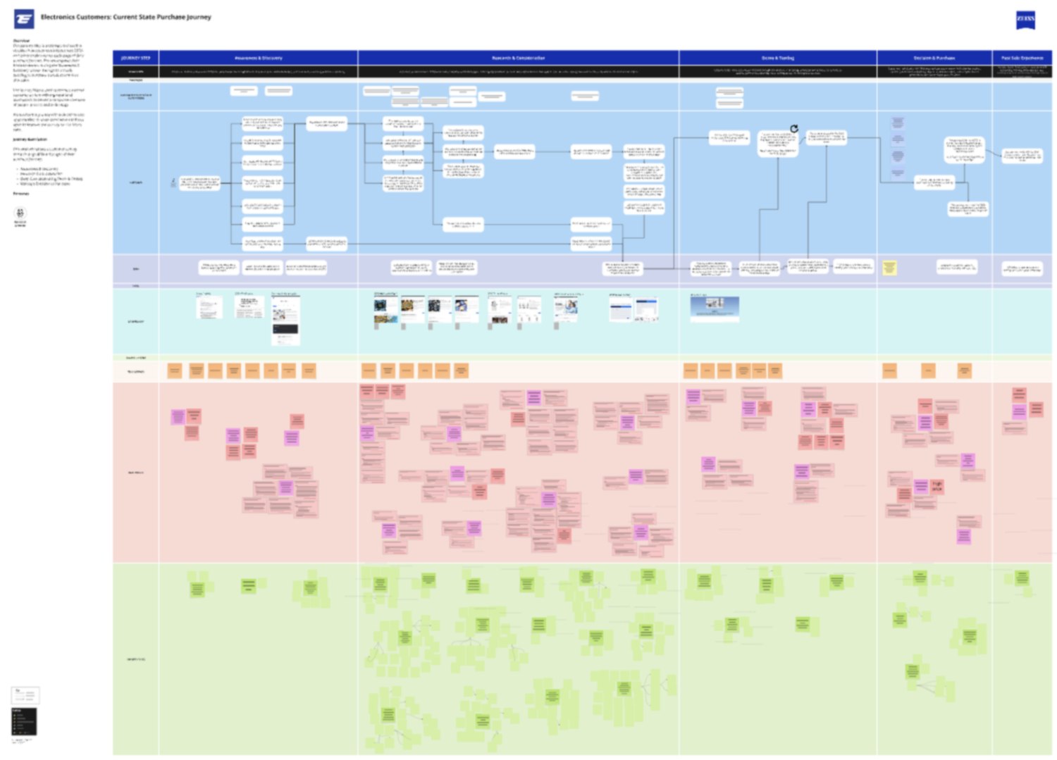
From those themes I built the current-state purchase journey blueprint: five stages from Awareness and Discovery through Research and Consideration, Demo and Testing, Decision and Purchase to Post-sale, with swimlanes for what the customer is thinking, what they do, the touchpoints and systems behind each step, and the pain points and opportunities sitting against them.
That fed the outputs deck I pulled together for the client — the key themes, what they meant for the journey, and the next steps worth taking. Phase one closed on an agreed proposal rather than an open question, which is what made a second phase straightforward to scope.
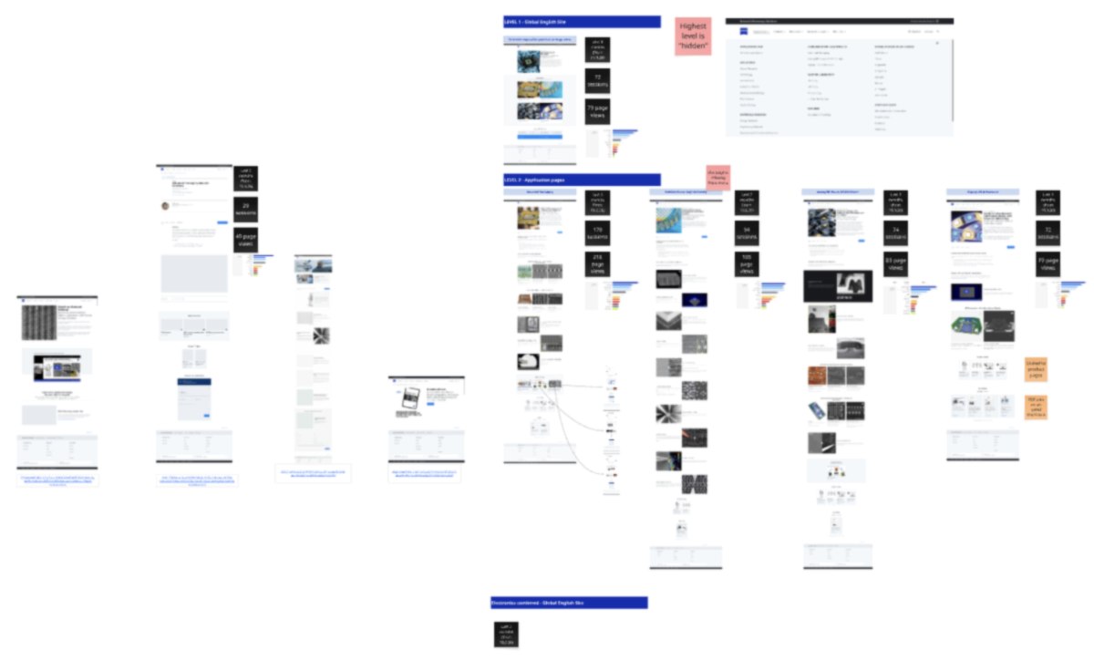
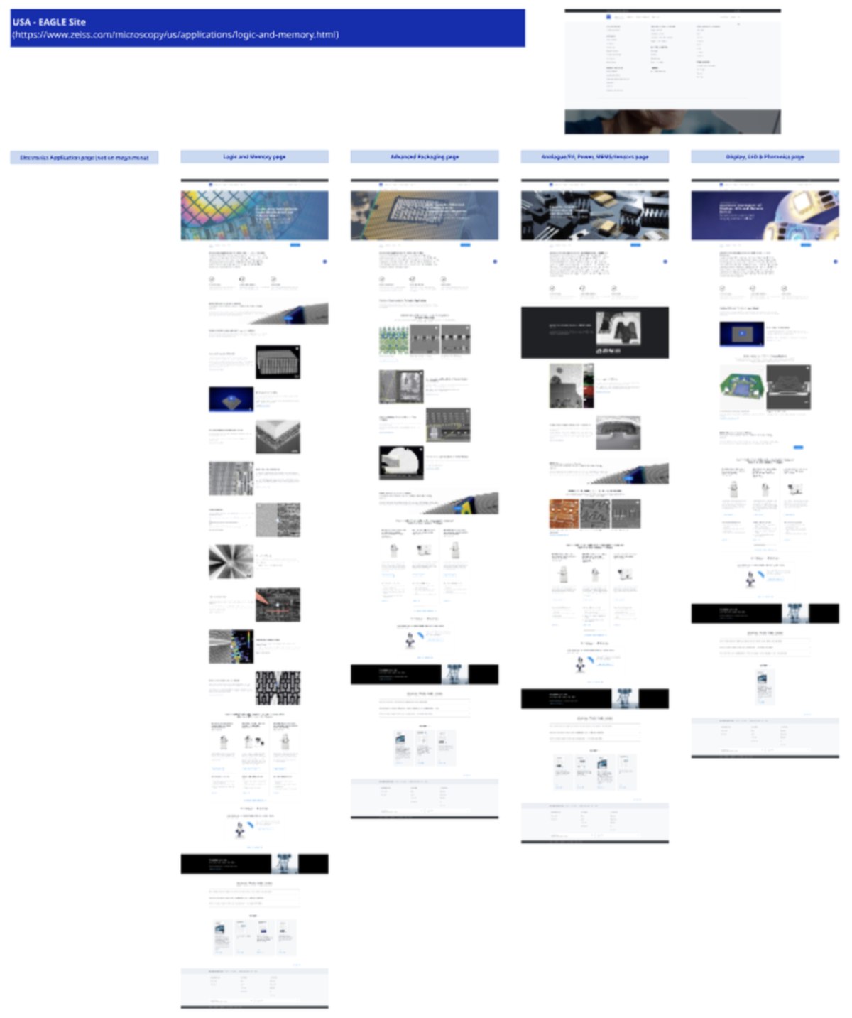
Phase two opened by mapping the journey again, this time against the website itself rather than the whole purchase — what a customer can actually reach, in what order, and where the path gives out.
That was done twice over, because the answer differed by market: the global English site and the US site each got their own current-state analysis, page by page, counting what was there and marking where the path ran out.
A colleague on the team ran a competitor analysis alongside it, which gave the recommendations something to be measured against: not just what was missing from the ZEISS journey, but what a customer in this market has already seen elsewhere and now expects.
Current-state analysis, global site (blurred)Current-state analysis, US site (blurred)
Phase two · An architecture organised by workflow
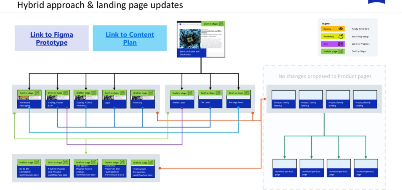
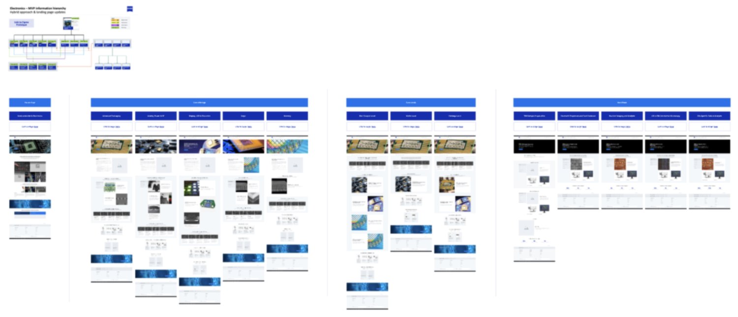
I facilitated the new information hierarchy spanning Electronics and Semiconductors. It is organised both by product family and, critically, by the workflow a customer arrives with — five workflow routes, each with its own steps, so routine imaging, failure analysis, correlative microscopy and sample preparation offer a way in that matches how the problem is framed in the customer’s head rather than in ZEISS’s catalogue.
Every product in the portfolio was mapped against those workflows and the workflows mapped onto the hierarchy, so the structure could be checked against the actual catalogue rather than agreed in the abstract and discovered to be wrong during the build.
The MVP information hierarchy (blurred)
Phase two · Prototypes, and the journey they produce
Working with our designer, I turned the hierarchy into draft pages — wireframes first, then an interactive prototype covering every page type, agreed with stakeholders page by page before any production work began. That sequencing is what stops a build stalling halfway through on a disagreement that should have surfaced in week three.
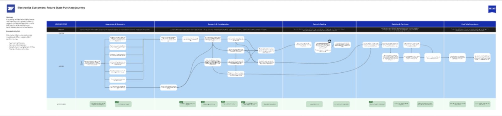
The future-state journey was mapped from the agreed pages, so the to-be was a description of something that existed and had been signed off rather than an aspiration drawn ahead of it.
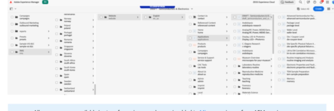
I worked with our AEM editor to get the pages built directly in the client’s experience platform, in parallel with content production and held together by a content plan and tracker so build, copy and imagery stayed aligned across fourteen pages.
The content plan was written to outlive the engagement. ZEISS finish the pages from it, which is why the last deliverable was a plan they could work through rather than a set of pages we had filled with placeholder text.
MVP pages in staging, ready for review (blurred)
Phase two · A configurator that knows its customer
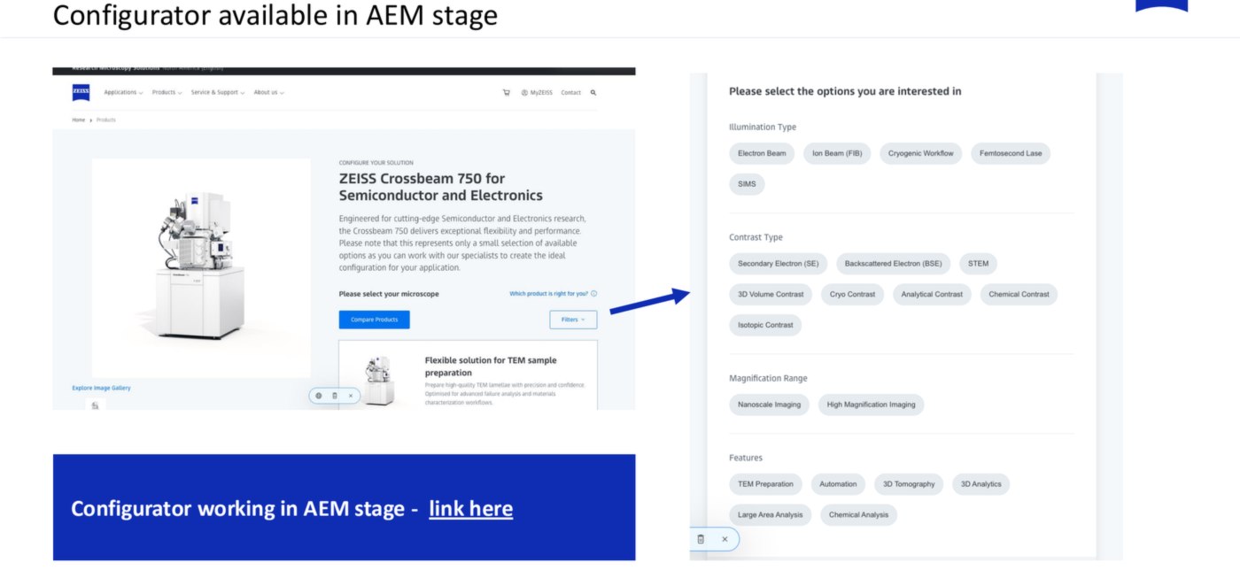
The product configurator was the point where the journey kept collapsing back into the generic. A customer could follow an electronics workflow all the way through and then land on a Crossbeam 750 configurator that was not specific to electronics at all — so the last step undid the specificity of every step before it.
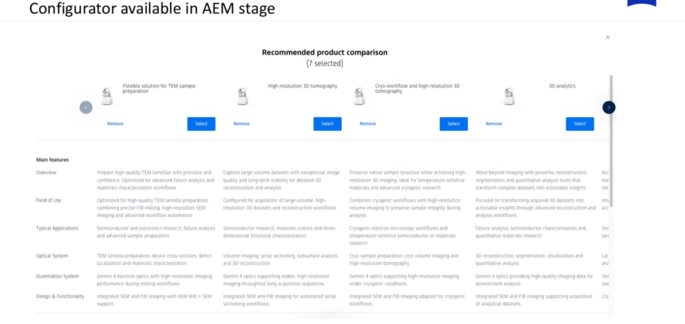
I worked on the changes that gave the Electronics portfolio a configurator of its own — the only one in scope here — with the options, illumination and detector types, magnification range and analysis features framed for this customer, so the journey ends on a product specified for the work they came to do. That ran alongside recommended-product comparison, filters and bundling, and I captured the draft requirements and worked with the technical team to close the content and specification gaps it depended on.
The electronics configurator in stagingRecommended product comparison
Outcome
A working MVP, and a route to the rest
14MVP pages liveBuilt in staging, ready for review
6 monthsEnd to endDefinition through to a build customers could use
The engagement produced an agreed future-state journey, a new information architecture spanning both portfolios, signed-off prototypes for every page type, and fourteen MVP pages built and live in staging — plus a content plan and tracker, an electronics-specific configurator, and a phased roadmap running from MVP through to full experience transformation.
What makes it a useful case rather than a website project is the model: interviews and a blueprint that locate the problem, an architecture organised around how customers describe their work rather than how the business files its products, prototypes agreed before a line of production code, and a build the client can carry on themselves. That is repeatable across any technically complex, multi-audience B2B portfolio.